Level 17: Anatomy of a Decoder
Open the level →Where it fits in the machine →
Task
Goal: build the recognition logic for 3 opcodes (ADD, STA, JMP) in the decoder: LED indicators on the outputs show which line is active.
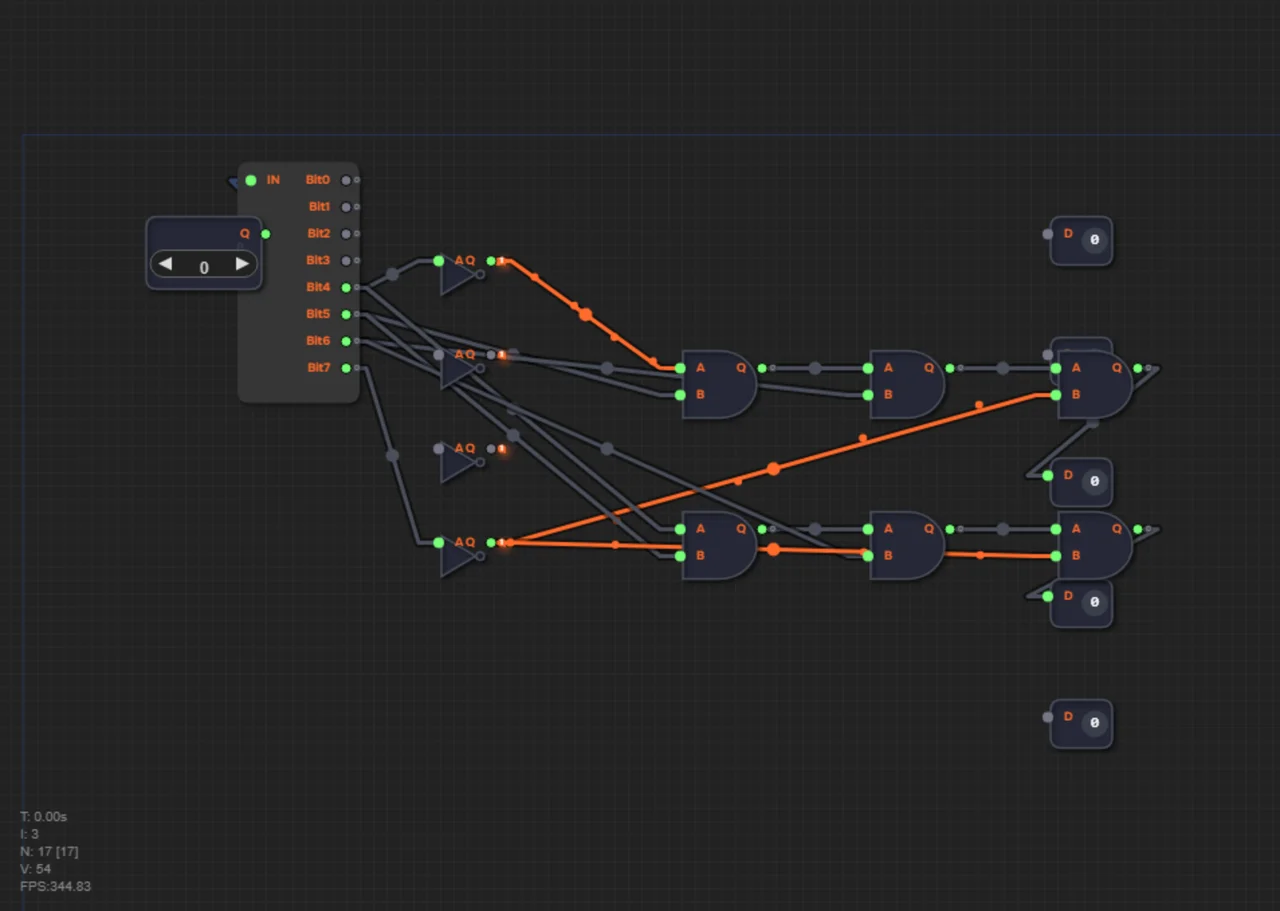
The instruction decoder turns an instruction code into control signals. The canvas already has a skeleton: - Splitter (pre:spl) — splits the input bus Instr into 8 bits. - 4 NOT inverters: ~Bit0 (pre:not0), ~Bit1 (pre:not1), ~Bit2 (pre:not2), ~Bit3 (pre:not3).
The main idea: an opcode is just bits, and recognizing it means ANDing the needed bits with negations of the others: each instruction activates exactly one decoder line. Along those lines the processor's control signals will flow later.
Path to this level
The competencies this level develops and their formation levels.
Related Materials
- Decoder: instruction decoder
Solution for self-check
Try building the circuit yourself first. The solution below is a way to check yourself if you're stuck or have already solved it.
What you should get: with Instr=0x60 (STA) MemWr lights up, with Instr=0x70 (JMP) — JumpUncond; on other opcodes the outputs stay silent.
The Instr input is a byte; bits 4–7 hold the operation: - ADD = 0001 (opcode 1, hex 0x10). - STA = 0110 (opcode 6, hex 0x60) — memory write. - JMP = 0111 (opcode 7, hex 0x70) — unconditional jump.
Recognizing an opcode means AND-ing four conditions: where a 1 is expected, connect the direct bit; where a 0 is expected, the inverted one (NOT turns 0 into 1 and "confirms" the match). A single AND accepts only 2 inputs but four bits must be checked, so each opcode needs a chain of three ANDs.
- STA (0110) → MemWr output. Fires when Bit0=0, Bit1=1, Bit2=1, Bit3=0:
- AND#1: input A = pre:not0 (~Bit0), input B = Splitter.Bit5 (Bit1 of the opcode).
- AND#2: input A = AND#1 output, input B = Splitter.Bit6 (Bit2).
- AND#3: input A = AND#2 output, input B = pre:not3 (~Bit3). Connect AND#3 output to MemWr.
- JMP (0111) → JumpUncond output. Fires when Bit0=1, Bit1=1, Bit2=1, Bit3=0:
- AND#4: input A = Splitter.Bit4 (Bit0 of the opcode), input B = Splitter.Bit5 (Bit1).
- AND#5: input A = AND#4 output, input B = Splitter.Bit6 (Bit2).
- AND#6: input A = AND#5 output, input B = pre:not3 (~Bit3). Connect AND#6 output to JumpUncond.
- ADD (0001) → all outputs 0. Leave ALUOp0, ALUOp1 and JumpCond unconnected: an unconnected Output is always read as 0.
The metaphor is a lock and key: an AND chain opens for exactly one bit pattern, like a lock opens for one key. Processor control signals will later travel along these lines.
Check yourself
Why does an opcode need a chain of three ANDs instead of a single gate?
AND accepts only 2 inputs but 4 bits must be checked: three ANDs gather a conjunction of four conditions.