Level 18: FINALE: The Ershov Computer
Open the level →Where it fits in the machine →
Task
Goal: build an 8-bit computer — Harvard architecture: ROM (instructions) + RAM (data) + PC + Register + ALU + Decoder + Clock.
The final level — build a complete 8-bit computer with Harvard architecture!
The main idea: a processor is not a new part but a joining of blocks already built: the ROM holds the program, the PC steps through instructions, the decoder interprets them, the ALU and accumulator compute. Your computer runs on the same logic built since level one.
Path to this level
The competencies this level develops and their formation levels.
Related Materials
- RAM: data memory
- ROM: instruction memory
- ProgramCounter
- Decoder: instruction decoder
- Assembler Manual
- How a Processor Works: From Transistor to Program
Tracing One Instruction
The circuit is built — now walk through it alongside a single instruction. Take LDA 5: "read cell 5 of the data memory into the register". Suppose RAM[5] holds the number 42 and the instruction is stored in ROM at address 3 — the program counter is currently 3.
- Where the instruction lives. A tick of Clock — and the program counter puts the number 3 onto the address input of ROM. Cell ROM[3] outputs the instruction byte.
- How the instruction is taken apart. The Splitter cuts the byte in half: bits 4–7 hold the operation code (for LDA), bits 0–3 hold the operand, the number 5.
- How the instruction is recognized. The Decoder receives the operation code and turns on exactly one output — the LDA line. All the other lines (ADD, STA, JMP) stay silent. This is the same "combination lock" from level 17.
- What data is read. The operand 5 goes to the address input of RAM. The data memory at address 5 puts the number 42 onto the bus.
- What changes in the register. The LDA signal switches the MUX at ALU input A — the same selector from level 9 — to the constant 0. The adder then passes the RAM data from input B, and after the clock edge the register holds 42: the path RAM → bus → ALU.B → ALU → Register8.
- Why PC moves on. No jump signal is active: the constant 1 at the adder input gets added to the counter, and after the tick PC = 4 — the processor is ready to fetch the next instruction.
Walk this path once more yourself — with your mouse across your own circuit, from ROM to Register8. Once you can tell the story without hints, try predicting the next step: what changes for STA 6 when the register already holds 42? Which decoder line fires, and where does the bus go this time? Check your prediction by running a three-instruction program: LDA 5, STA 6, HLT.
What happens to your program: from code to bytes
The "Assembler" tab on this level opens with a ready-made program already in the editor (and the gray template in an empty editor is just a hint, not code). Lines starting with ; are comments — the assembler skips them; they exist only for you. Here is what happens to the program after you press "Run".
The assembler turns each line of the program into a single byte and writes the bytes into ROM one after another, starting at address 0. In each byte, bits 4–7 hold the operation code (ADD = 1, LDA = 5, STA = 6, HLT = 15), bits 0–3 hold the operand. These are the bytes your circuit then takes apart: the Splitter peels off the opcode for the decoder, the operand goes to the RAM address input or into the ALU.
An example program with comments:
; LDA and ADD read RAM at the address taken from the operand
LDA 5      ; byte 0x50: ACC = RAM[5]
ADD 3      ; byte 0x13: ACC = ACC + RAM[3]
STA 0      ; byte 0x60: RAM[0] = ACC
HLT        ; byte 0xF0: the processor stops
After pressing "Run", four bytes land in ROM: 50 13 60 F0 (hexadecimal — visible in the ROM editor). Run the ticks, and this path should go through your circuit: PC=0 → ROM outputs 0x50 → the decoder turns on the LDA line → the value of RAM[5] lands in the register; then ADD adds RAM[3], STA writes ACC into RAM[0], and HLT stops the clocking. Expected result: the register (ACC) holds RAM[5] + RAM[3], RAM[0] holds the same result, and the program counter freezes at address 4 (with RAM[5]=5 and RAM[3]=3 that is ACC = 8, RAM[0] = 8). The debug panel under the editor shows PC, ACC and RAM contents — handy for checking every tick.
The level check makes sure it is your circuit that executes the program: the blocks are in place, Clock is connected to PC, RAM writing is enabled, and the program in ROM actually runs through the ticks.
Solution for self-check
Try building the circuit yourself first. The solution below is a way to check yourself if you're stuck or have already solved it.
The in-game hint on this level inserts a scaffold: the circuit without two wires — Clock to the program counter and the RAM write line. Connect them yourself: without them the processor never ticks and never remembers — the two key principles of the final level.
What you should get: after running the preloaded program (LDA 5, ADD 3, STA 0, HLT) the register (ACC) holds RAM[5] + RAM[3], RAM[0] holds the same result, and the program counter freezes at address 4. With RAM[5]=5 and RAM[3]=3 that is ACC = 8, RAM[0] = 8.
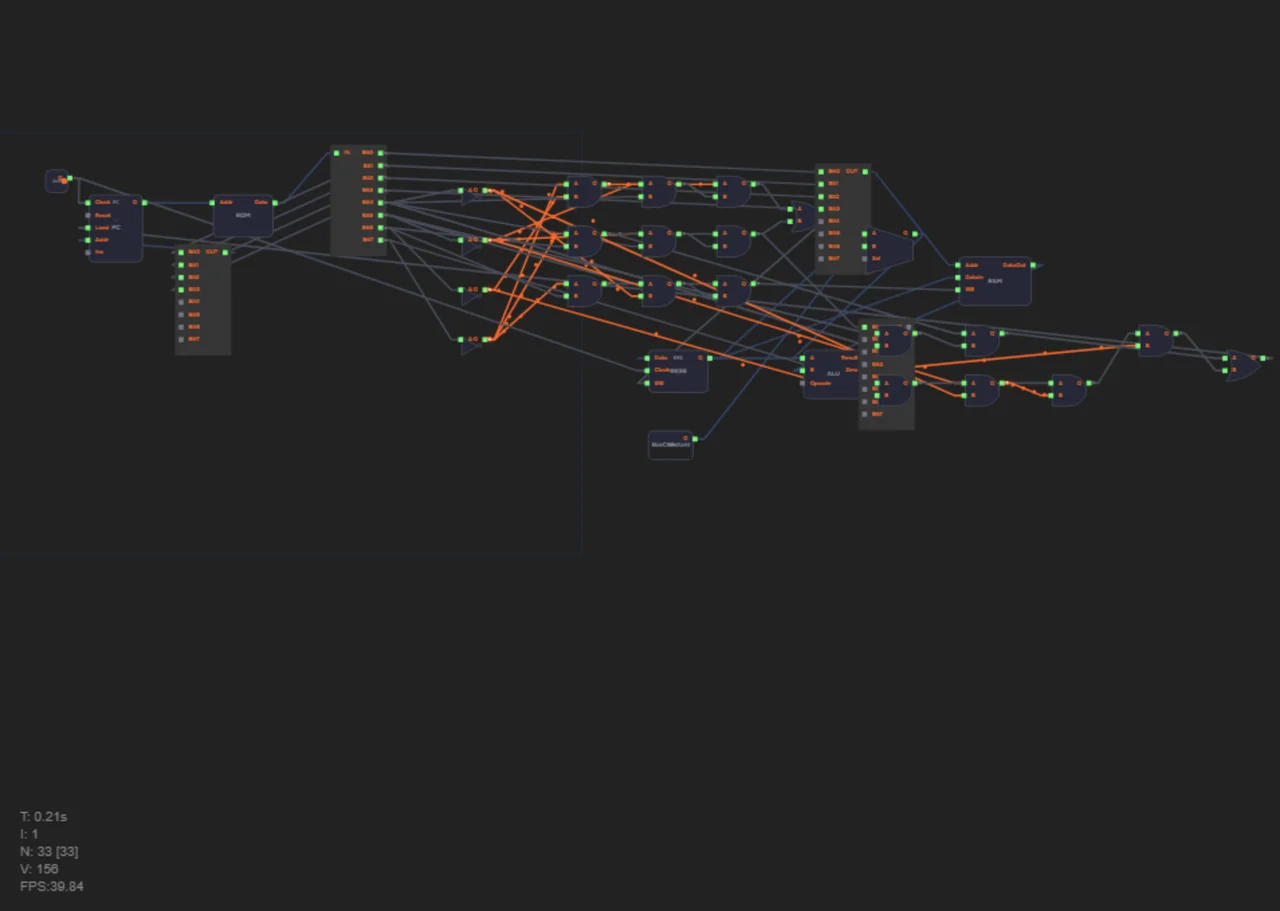
Main processor cycle: Clock → PC (program counter) → ROM (instruction memory) → Decoder → Register + ALU → RAM (data memory). Instead of Register8 you can use your Register chip — the level 12 reward; it is the same register.
- ProgramCounter — a ready-made block from the palette. Feed the PC output to the address input of ROM.
- ROM — instruction memory (256 bytes): Addr input receives the address from PC, Data output gives the instruction byte.
- Splitter — split the ROM output into two parts: bits 4–7 → Opcode (the command code), bits 0–3 → Operand (the address or value).
- Decoder — recognizes the Opcode and produces 5 control signals. There is no ready-made "Decoder" block in the palette on this level — build it from NOT and AND gates (the checkpoint requires at least 2 NOT and 2 AND), like the "combination lock" of level 17: for the right bit pattern exactly one line fires.
- ADD — the ALU adds (the register captures the result).
- LDA — the multiplexer puts 0 on ALU input A, so the adder passes the RAM data through to the register.
- STA (MemWr) — RAM write enable.
- JMP — unconditional jump.
- JZ — conditional jump (ALU result = 0). For jumps: PC.Load = JMP OR (JZ AND Zero), where Zero is the zero flag from the ALU output.
- Register8 — holds the intermediate result. Data comes from the ALU output or RAM.
- ALU — performs operations on the operand and the register.
- RAM — data memory (256 bytes): reads and writes data at the address taken from the instruction operand.
After assembly, open the "Assembler" tab — the commented program is already prepared in the editor (the assembler skips lines starting with ;). Press "Run" and run the clock ticks. Expected result: ACC = RAM[5] + RAM[3], RAM[0] = ACC; with RAM[5]=5 and RAM[3]=3 that is ACC = 8, RAM[0] = 8.
Check yourself
Why does LDA read data from RAM rather than ROM?
ROM stores the program (instructions), RAM — the data. The LDA operand is a data cell address: the value travels through the bus and the ALU MUX into the accumulator.