All 41 simulator components on one page: a real canvas snapshot of each component, a short description, and a link to a datasheet with the truth table. Come back here whenever you meet an unfamiliar circuit element.
Besides the palette elements, a circuit you build can be folded into a custom chip — a ready-made block with propagation delay, like a real IC. The first reward chip is the ADDER8 8-bit adder; the rest are awarded for levels 13–16 and part finals.
Basic logic
Component
Description
Datasheet
NAND
A universal logic gate. Outputs 0 only when both inputs are 1; all other cases yield 1. Any other logic gate can be built from NAND gates: NOT, AND, OR, XOR, and even an entire processor.
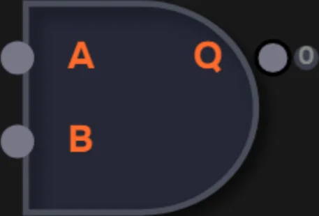
Logical multiplication (conjunction). Outputs 1 only when both inputs are 1, otherwise 0. Matches the "AND" operation: result is true only if both conditions are true.
Logical addition (disjunction). Outputs 1 if at least one input is 1. Only outputs 0 when both inputs are 0. Matches the "OR" operation: result is true if at least one condition is true.
Combination of OR and NOT. Outputs 1 only when both inputs are 0; all other cases yield 0. Used as the foundation for RS latches and other memory circuits.
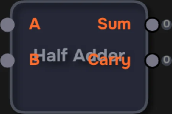
Adds two bits. Produces a sum (Sum) and a carry (Carry). Cannot handle a carry from a previous bit — that requires a Full Adder. Built from XOR and AND.
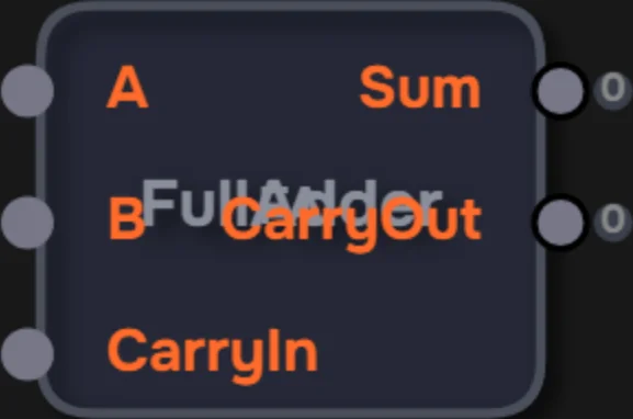
Adds three bits: two operands plus a carry from the previous bit (CarryIn). Produces a sum (Sum) and a carry (CarryOut). Chaining multiple Full Adders enables multi-bit arithmetic.
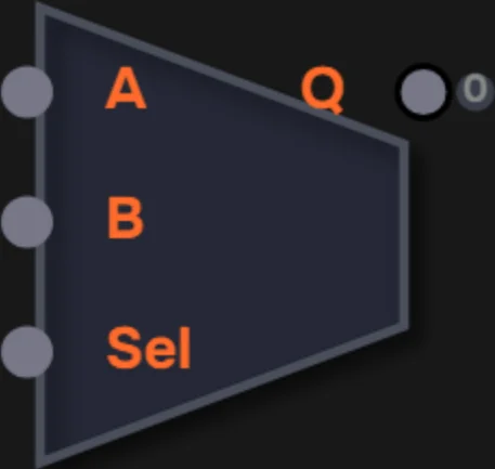
Routes one of two input signals to the output depending on a selector signal. If selector = 0, the first input passes through; if 1 — the second. Acts as a digital switch.
Sets a numeric value from 0 to 255 on an 8-bit data bus. Value is set with a slider. The bus combines 8 bits into one number — a convenient way to work with bytes.
Shifts an 8-bit value one bit to the left: each bit moves to a more significant position, bit 7 is dropped, and 0 is written into bit 0. Arithmetically this multiplies by 2 (modulo 256).
Shifts an 8-bit value one bit to the right: each bit moves to a less significant position, bit 0 is dropped, and 0 is written into bit 7. Arithmetically this is integer division by 2.
Stores one bit of data. The output (Q) changes only at the rising edge of the clock signal. Between edges, the output holds the previous value. The basic building block for registers and counters.
Stores one byte (8 bits). Writes a new value on the clock edge. Until the next clock edge, the register holds the previous value. Used for temporary data storage in the processor.
Stores 256 bytes of data that do not change during operation. Addressed by an 8-bit address (0–255). Contains the processor program or constants. Data is retained even when power is off.
Stores 256 bytes of data with read and write support. Addressed by an 8-bit address. Data is temporary — lost on power-off. Used for storing variables and computation results.
Holds the address of the currently executing instruction. On each clock cycle it increments by the Inc value (default 1), advancing to the next instruction. The most critical part of the processor — determines which command to fetch from memory.
Index register for indirect addressing. Stores an 8-bit address used to access arrays in RAM. Increments by 1 on Clock edge when Inc=1. Loads data from bus when WE=1.
Address decoder. Determines whether an address belongs to RAM (0x00–0xDF) or I/O devices (0xE0–0xFF). Generates signals to arbitrate access between RAM and I/O devices.
Linear Feedback Shift Register — an 8-bit pseudorandom number generator. Polynomial: x^8 + x^6 + x^5 + x^4 + 1. Shifts on every Clock edge. Read via port 0xFA (DevAddr=0x1A).
Splits an 8-bit instruction into two fields: the upper 4 bits are the opcode, the lower 4 bits are the operand. Based on the opcode it generates 9 control signals that enable the right processor blocks: register write, RAM read, ALU operation selection, jumps.
Second-generation instruction decoder: same protocol (opcode [7:4], operand [3:0]), but 12 control signals instead of 9. JZ and JN have separate outputs, and two new signals were added: ACC_WE (accumulator write enable) and ImmOp (immediate operand select).
Performs 8 operations on two 8-bit numbers: ADD, SUB, AND, OR, XOR, NOT, SHL (shift left), SHR (shift right). The operation is selected by a control signal. The heart of any processor.
Generates a periodic signal that toggles between 0 and 1 at a set frequency. Used to synchronize sequential circuits: registers, counters, memory, and the entire processor.
A manual clock signal generator. Each press of the «▶ Tick» button produces a full clock pulse (0→1→0) on the Tick output. Used for step-by-step manual clocking of a circuit.
A signal receiver. Displays the current value (0 or 1) on its input. Serves as the circuit's output port — its value is checked against the truth table to verify correctness.
A 4-button gamepad (Up/Down/Left/Right) for controlling circuits and programs. Addressed via port 0xFE (DevAddr=0x1E). Returns a bitmask of pressed buttons.
Shows the numeric value on its input in decimal, binary, or hexadecimal format. Switch modes by clicking on the display. Indispensable for debugging and visualizing circuit behavior.
 NAND
NAND
 NOT (Inverter)
 AND
AND
 OR
OR
 XOR (Exclusive OR)
 NOR
NOR
 Half Adder
 Full Adder
 MUX (Multiplexer 2→1)
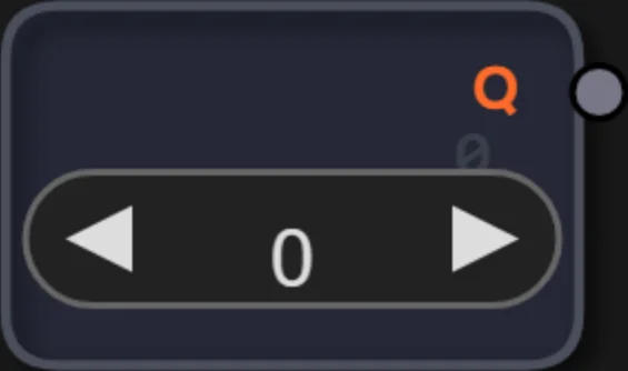 Bus Input (8-bit)
 Bus Output (8-bit)
 Bus Constant
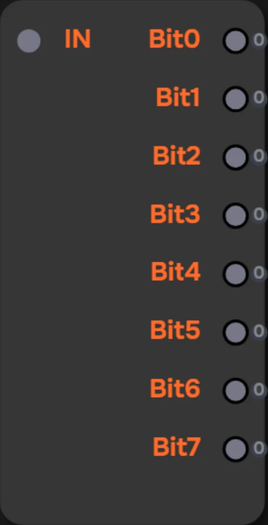 Splitter (bus→bits)
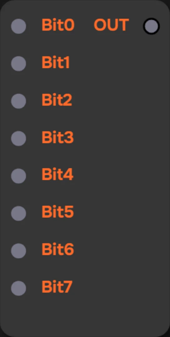 Maker (bits→bus)
 Bus NOT
 Bus AND
 Bus OR
 Bus XOR
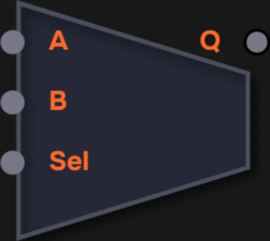 Bus MUX
 Bus SHL
 Bus SHR
 Bus Zero (zero detector)
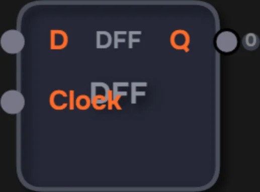 DFF (D Flip-Flop)
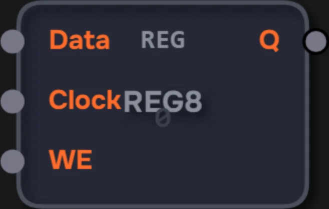 Register 8-bit
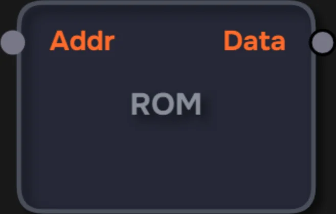 ROM (Read-Only Memory)
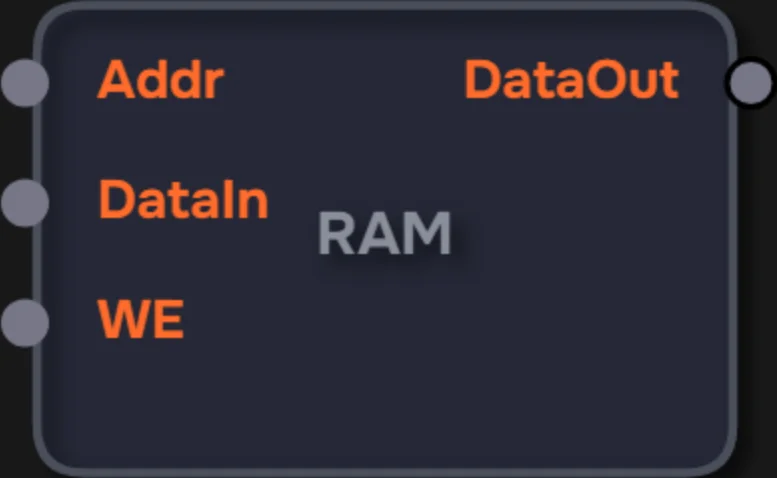 RAM (Random Access Memory)
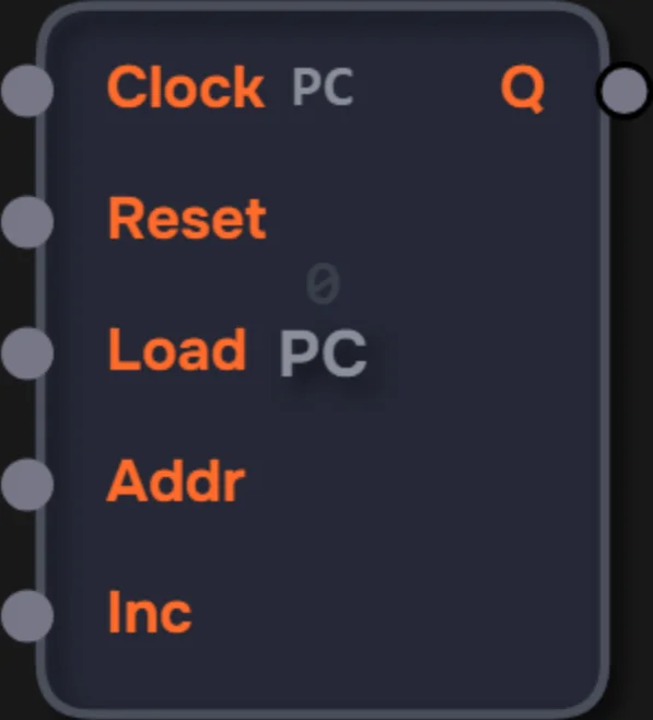 Program Counter
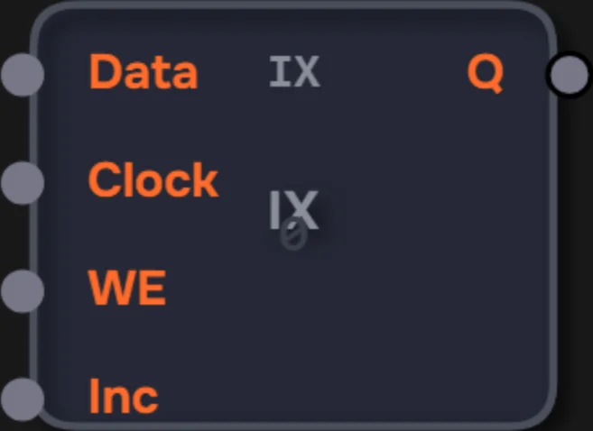 Index Register (IX)
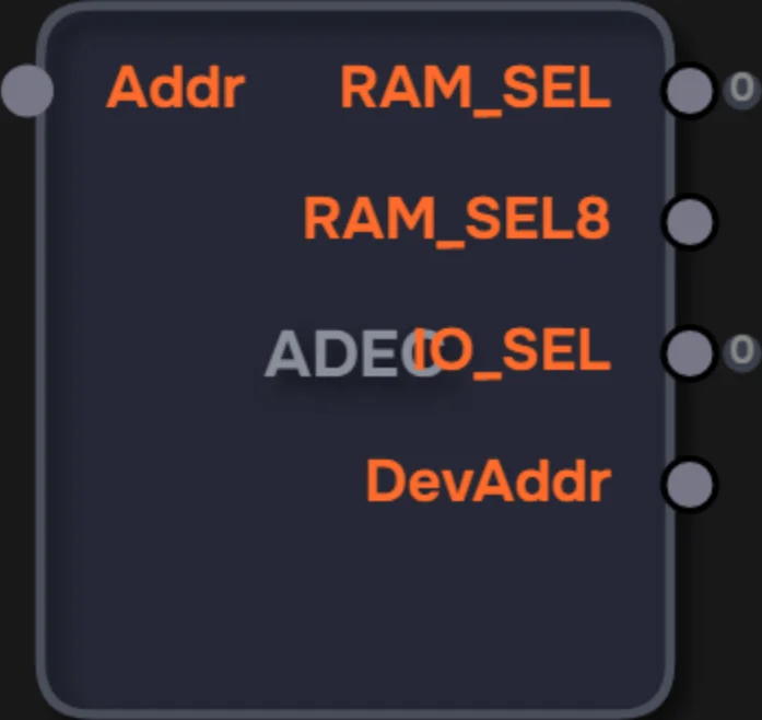 Addr Decoder (ADEC)
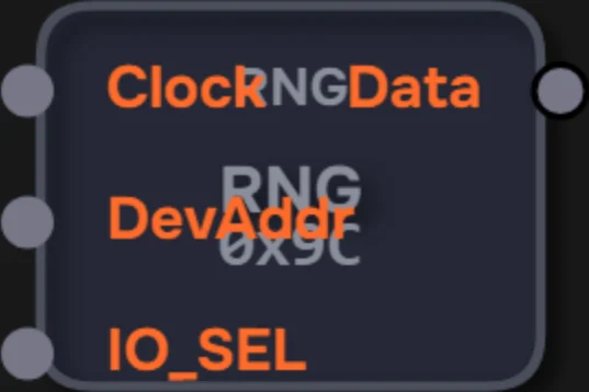 LFSR (Random Number Generator)
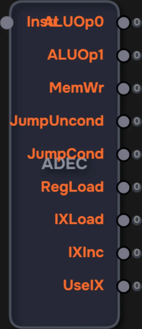 Decoder (instruction decoder)
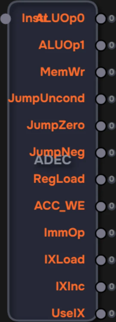 Decoder V2 (instruction decoder V2)
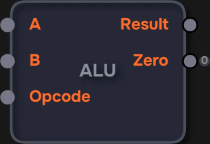 ALU 8-bit (Arithmetic Logic Unit)
 Clock
Clock
 Manual Clock
 Input
Input
 Output
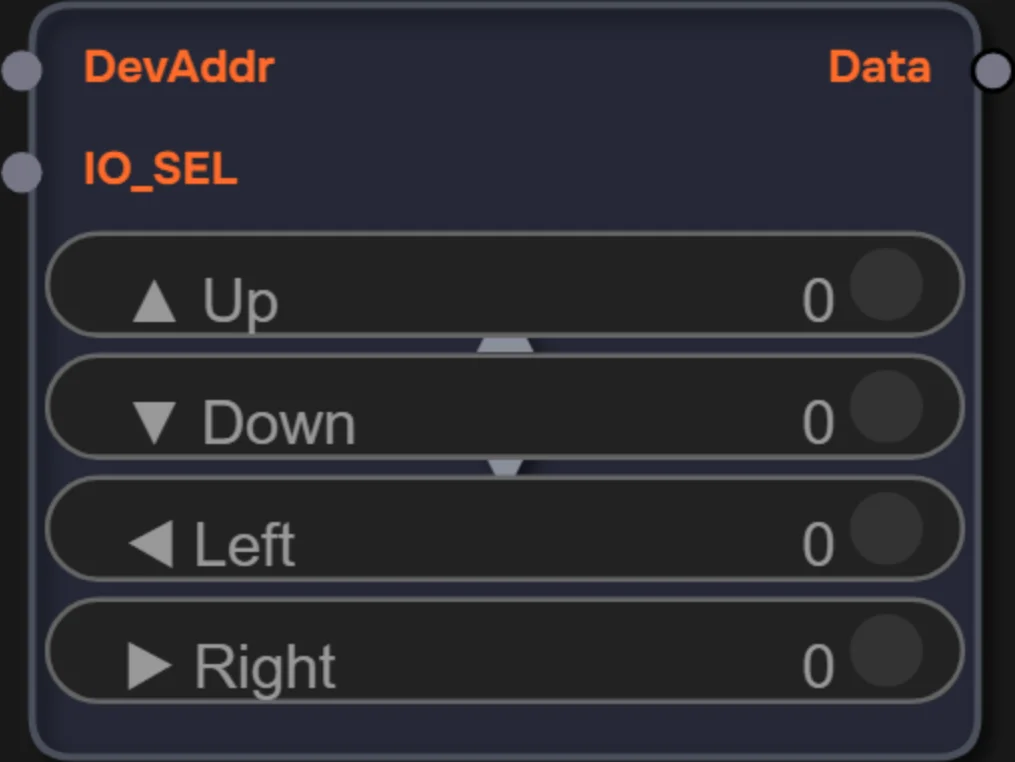 Gamepad
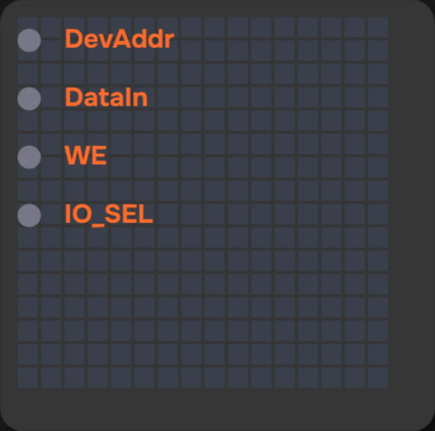 Matrix Display 16x16
 Display
 LED8 (LED bar)