Verilog: Memory and Time — Flip-Flops, Registers, RAM
So far in the "From Code to Silicon" series every circuit has been an honest egoist of the present: its output depended only on the current inputs. No matter how much you wiggle the inputs, the circuit will not remember what happened a second ago. Memory appears at the moment time enters the circuit: the clock signal and the D flip-flop. Levels 3.37–3.39 add exactly that ability — and with it almost everything that separates a processor from a calculator.
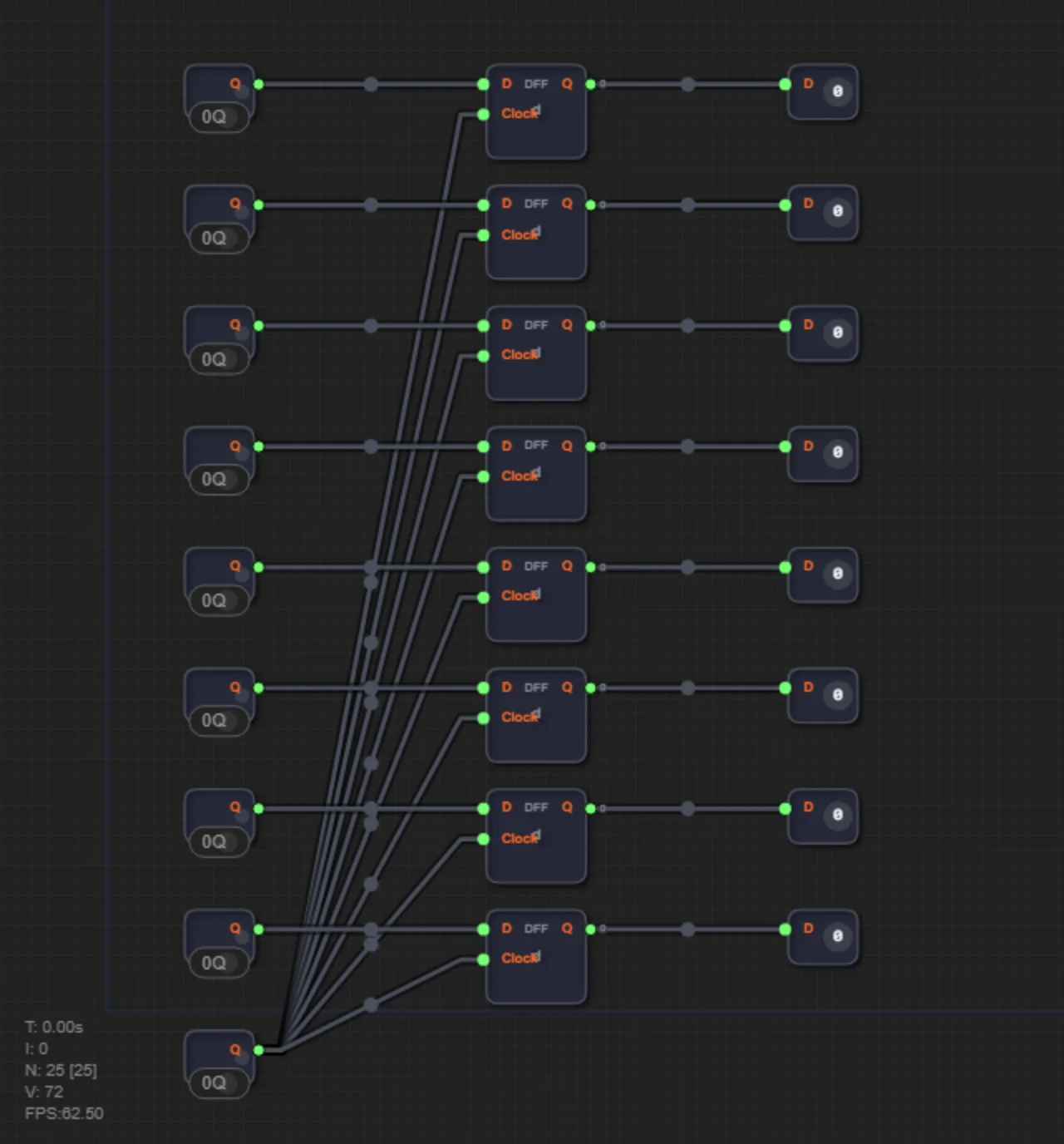
Time in a circuit: the dff primitive
The D flip-flop is the only primitive in the course that "lives" in time. Its rule: on the clock edge (clk going 0 → 1) the flip-flop captures what is on input D at that moment and holds it on output Q until the next edge. Between edges, any changes on D are ignored.
In structural Verilog a flip-flop is a primitive just like and or not:
module bit_latch(input d, input clk, output q);
  dff cell(q, d, clk);
endmodule
The key idea level 3.37 checks: the clock is not a "refresh button" but the boundary between the circuit's past and future. Everything combinational (gates) lives within a tick; everything sequential (dff) jumps across the edge.
A register: eight flip-flops in one line
An 8-bit register is simply eight dff cells with a shared clock, each holding its own bit. Writing eight lines and wiring them by hand is unnecessary: Verilog can unroll identical constructs with a generate-for loop — the very feature you mastered on level 3.37:
module reg8(input [7:0] d, input clk, output [7:0] q);
  genvar i;
  generate
    for (i = 0; i < 8; i = i + 1) begin : bits
      dff cell(q[i], d[i], clk);
    end
  endgenerate
endmodule
The loop turns into eight separate flip-flops at the circuit "assembly" stage — hardware does not know loops; they exist only for writing convenience. On level 3.38, "Step by Step", the register already works together with an adder: each tick the counter gets a step added — that is how a program counter, the heart of any processor, is born.
RAM256: memory with an address
The next step is storing not one byte but hundreds. RAM256 is a course built-in module: 256 cells of one byte each, accessed via an 8-bit address. Writing: present the address and data, raise the write signal — on the clock edge the value lands in the cell. Reading: present the address — the output shows the contents.
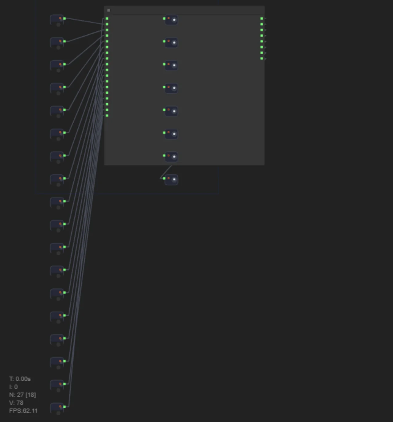
On level 3.39 the RAM256 is given as a ready "black box" — your task is the combinational logic around it: decoding the read/write mode and routing the buses. This very block later becomes the data memory of the level 3.40 processor, "CPU Heart": ROM holds the program, RAM holds the data — and the Harvard separation described in the architecture article gains its real wires.
What's next
Flip-flop + register + RAM + a clock — that is the full kit for a circuit to "come alive". Level 3.40 assembles them into a processor with a program, and you are ready to read its circuit in the RTL viewer and understand every block. How to take the project all the way to a real Tang Nano 9K board — that is the next article in the series.
Test yourself
When exactly does a dff capture input D?
On the clock edge — the moment clk goes from 0 to 1. Between edges, changes on D have no effect.
Into how many Verilog constructs does the generate-for of reg8 unroll?
Eight dff instances — one per bit. The loop exists only in the source text; in hardware it is eight independent flip-flops with a shared clock.
Why is RAM256 addressed by exactly eight bits?
Eight bits give 256 combinations — exactly one per cell of a 256-byte memory.