Level 46: Memory-Mapped I/O
Task
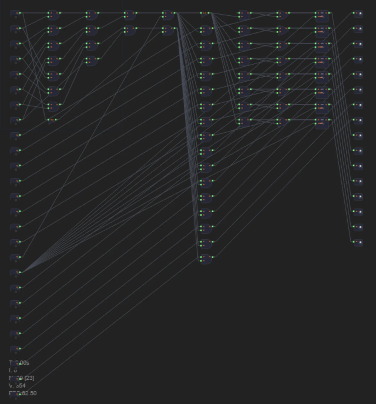
Implement a memory-mapped I/O controller. The IOController module connects to the processor's address and data bus:
- Write to address 0xFF (addr=0xFF, we=1) — stores data_in in the led_out register, lighting the LEDs.
- Read from address 0xFE (addr=0xFE, we=0) — outputs the switch states switches_in to data_out.
Use generate-for for the 8-DFF array and AND-trees for address decoding. The interface will show a "Peripherals" panel with 8 LEDs and 8 switches.
Related materials
- RAM — memory and addressing
- Data Buses in Verilog — 8-bit connections
Solution for self-check
Try building the circuit yourself first. The solution below is a way to check yourself if you're stuck or have already solved it.
The controller has four parts:
- 0xFF address detector: AND-tree of all 8 addr bits → addr_ff. Write strobe:
wr_en = addr_ff AND we. - led_out register: generate-for (i=0..7) with DFF and hold logic: when wr_en=1, load data_in[i]; otherwise hold current led_out[i].
- 0xFE address detector: addr[7:1]=1, addr[0]=0 → addr_fe.
- data_out output: generate-for (j=0..7):
data_out[j] = switches_in[j] AND addr_fe(when addr_fe=1, output switches; otherwise 0).
module IOController(
    input wire [7:0] addr,
    input wire [7:0] data_in,
    input wire we,
    input wire clk,
    input wire [7:0] switches_in,
    output wire [7:0] data_out,
    output wire [7:0] led_out
);
  // 0xFF detector
  wire t0, t1, t2, t3, t4, t5, addr_ff;
  and a1(t0, addr[0], addr[1]);
  and a2(t1, addr[2], addr[3]);
  and a3(t2, addr[4], addr[5]);
  and a4(t3, addr[6], addr[7]);
  and a5(t4, t0, t1);
  and a6(t5, t2, t3);
  and a7(addr_ff, t4, t5);
  wire wr_en, wr_not;
  and aw(wr_en, addr_ff, we);
  not nw(wr_not, wr_en);

  // 0xFE detector
  wire fe_a1, fe_a2, fe_a3, fe_a4, fe_a5, fe_hi, addr_0n, addr_fe;
  and b1(fe_a1, addr[1], addr[2]);
  and b2(fe_a2, addr[3], addr[4]);
  and b3(fe_a3, addr[5], addr[6]);
  and b4(fe_a4, fe_a1, fe_a2);
  and b5(fe_a5, fe_a3, addr[7]);
  and b6(fe_hi, fe_a4, fe_a5);
  not b7(addr_0n, addr[0]);
  and b8(addr_fe, fe_hi, addr_0n);

  // LED register
  generate
    genvar i;
    for (i = 0; i < 8; i = i + 1) begin : led_gen
      wire t_on, t_hold, led_d;
      and d1(t_on, data_in[i], wr_en);
      and d2(t_hold, led_out[i], wr_not);
      or  d3(led_d, t_on, t_hold);
      dff dff_i(led_out[i], led_d, clk);
    end
  endgenerate

  // data_out
  generate
    genvar j;
    for (j = 0; j < 8; j = j + 1) begin : data_gen
      and gm(data_out[j], switches_in[j], addr_fe);
    end
  endgenerate
endmodule
The key insight: wr_not = NOT wr_en. When wr_en=1: led_d = data_in[i] AND 1 = data_in[i] (load). When wr_en=0: led_d = led_out[i] AND 1 = led_out[i] (hold). DFF captures led_d on the rising edge of clk.