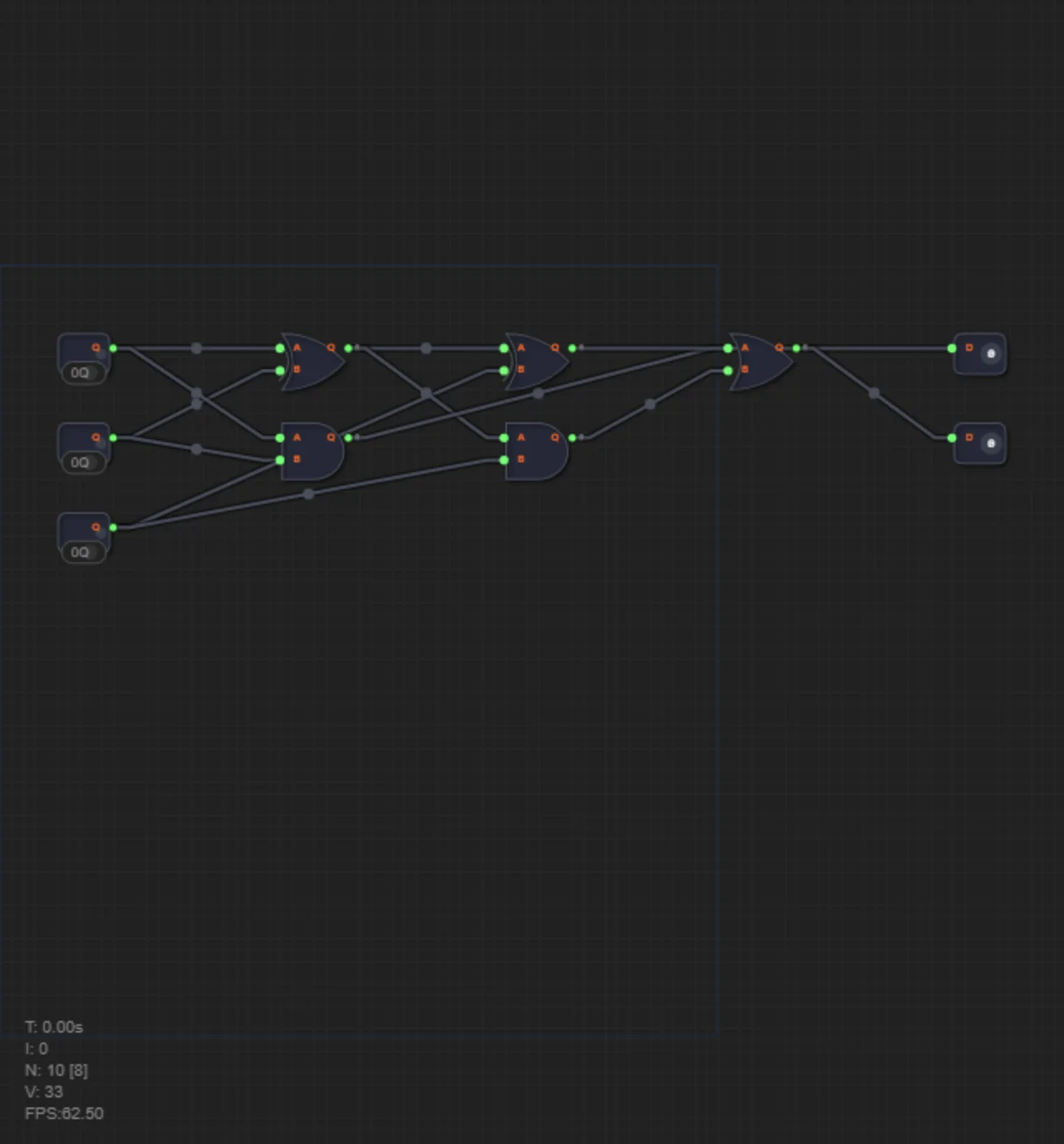
Level 43: Freezing Time
Task
The FullAdder module has a bug — one of the wires is connected incorrectly. Some tests fail. Find the error, fix it, and get all tests passing.
File fulladder.v is editable. cpu.v and testbench.v are read-only (context). Use the tabs to switch between files.
Hint: look closely at gate g4 — which signal should it process for correct carry generation c_out?
Related materials
- Full Adder — classical schematic
- Verilog Is Not Programming — thinking in circuits
Solution for self-check
Try building the circuit yourself first. The solution below is a way to check yourself if you're stuck or have already solved it.
How to read a waveform and find the bug:
1. Find the moment where the test result diverges from the expected one (the first mismatch on sum or c_out).
2. Look at the internal wires at that same moment — which signal behaves incorrectly.
3. Walk backwards from the output to the source: c_out → w2/w3 → gates → inputs. The bug always lives in the gate whose output does not match the formula.
See the Timing Diagram article.
In file fulladder.v, the error is in gate g4:
and g4(w3, w1, w2); // bug — third port is w2 instead of c_inFix:
and g4(w3, w1, c_in); // correct — w3 = w1 AND c_inSignal w3 contributes to the output carry: c_out = w2 OR w3, where w2 = a AND b. Full formula: c_out = (a AND b) OR ((a XOR b) AND c_in) — the classical full adder logic. Using w2 instead of c_in produces incorrect results.
One more detail the waveform reveals: values change between clock edges, and they are sampled at the edge. In sequential circuits (DFFs, registers) a value is captured exactly at the clock edge — anything that arrives late for the edge (like the delayed Carry in this level) will only reach the register on the next tick.