Instruction Decoder
Suppose the Program Counter has just fetched a byte of code — 10100111 — from memory. To us it's just a string of ones and zeros, but for the processor it's a command. Yet how do you make this command physically do work? How does the ALU know it should add, and how does RAM understand that data is about to be written to it?
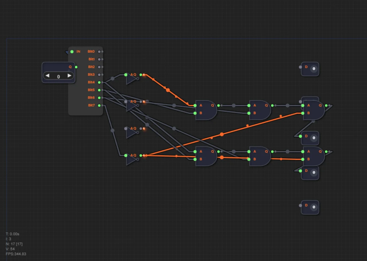
That's the job of the Instruction Decoder. It's a combinational circuit of logic gates that works like a perfect translator: it takes the binary operation code (opcode) on its inputs and instantly turns it into a set of control signals.
For example, the decoder sees the "Store to memory" code (STA). It immediately activates the wire leading to the Write Enable pin of the RAM chip and, at the same time, switches off all the other unneeded modules. The decoder is a real puppeteer: it pulls the right strings (wires), making the whole processor synchronously carry out the programmer's will.
What an instruction is made of
In our computer, an instruction byte is split in half: the upper 4 bits (bits 7–4) are the opcode — the operation code; the lower 4 bits (bits 3–0) are the operand, usually an address or a value. Four opcode bits give 24 = 16 possible instructions — exactly as many as our processor can encode.
On level 1.17 the decoder must "recognize" three commands: ADD = 0001 (0x10) — addition, STA = 0110 (0x60) — memory write, JMP = 0111 (0x70) — unconditional jump. The other codes are simply not used at this level.
Recognition through AND chains
How does the circuit know that the opcode equals 0110? For each command we build a chain of AND gates that outputs 1 only for one specific combination of bits. Since a single AND accepts only two inputs, checking four bits requires a chain of three ANDs.
In the game the opcode is taken from a Splitter: bits 4–7 of the byte are exactly the four command bits. To check that a bit equals zero, it first goes through a NOT inverter — four ready inverters are already placed on the canvas. How the instruction byte gets to the decoder at all is described in the article on the program counter.
Table: opcode → control signal
| Opcode | Command | Signals fired |
|---|---|---|
| 0001 (0x10) | ADD | No signals — the ALU adds by default (ALUOp = 00) |
| 0110 (0x60) | STA | MemWr = 1 — RAM write enable |
| 0111 (0x70) | JMP | JumpUncond = 1 — program counter overwrite |
In total the decoder has five outputs: ALUOp0 and ALUOp1 (ALU operation select), MemWr (memory write), plus JumpUncond and JumpCond (unconditional and conditional jumps).
A numeric example: decoding 0x60
Take the byte 0x60 = 0110 0000. The upper four bits — 0110 — are the STA opcode, the lower ones — 0000 — are the operand (address 0). Let's walk through how the decoder "recognizes" STA.
1. The Splitter breaks the byte into 8 bits; we're interested in bits 4–7: 0, 1, 1, 0.
2. To turn the zero bits into ones, pass them through NOT: ~bit0 = 1 and ~bit3 = 1.
3. Build the AND chain: (~bit0) AND bit1 AND bit2 AND (~bit3).
4. Substitute the values: 1 AND 1 AND 1 AND 1 = 1 — a one appears at the MemWr output!
5. The processor enables the RAM write: the byte from the accumulator goes onto the data bus and is stored at the address from the operand (0).
Notice: recognizing a zero requires an inverter — so the NOT gates are essential. On level 1.18 this decoder is embedded in a complete Harvard computer: ALUOp signals control the ALU, MemWr controls the memory, and JumpUncond and JumpCond go through an OR gate into the Load input of the program counter.
Decoding is instant and parallel
The whole magic of the decoder is that it's pure combinational logic: no clocks, no waiting. As soon as the instruction byte appears on the input, the signals on the outputs settle after the signal travels through a few gates — in a fraction of a tick. All five control lines are computed simultaneously, in parallel.
The "program counter → memory → decoder → execution blocks" chain is exactly the instruction execution cycle. How addresses and data travel over buses and why wires don't collide is described in the article "Bus Conflicts and the Address Decoder".
Common mistakes
- Checking only the ones: for bits that must be zero, an inverter is mandatory — otherwise the chain fires for several opcodes at once.
- Forgetting the three-AND cascade: a single AND accepts only two inputs, but four bits need checking.
- Mixing up the signals: STA activates MemWr, while JMP activates JumpUncond — not the other way around.
Summary
1. An instruction byte = opcode [7:4] + operand [3:0]; four opcode bits encode up to 16 commands.
2. The decoder is a combinational circuit that turns an opcode into control signals.
3. In the game the opcodes ADD (0x10), STA (0x60), and JMP (0x70) are recognized by AND and NOT chains.
4. STA fires MemWr (RAM write), JMP fires JumpUncond (PC overwrite), and ADD fires nothing — the ALU adds by default.
5. The decoder has five outputs: ALUOp0, ALUOp1, MemWr, JumpUncond, JumpCond.
6. On level 1.18 the decoder becomes part of the complete Ershov Computer.
In levels 1.17–1.18 you will first build the recognition logic for three opcodes from AND and NOT chains, and then embed the ready decoder into the complete Ershov Computer.