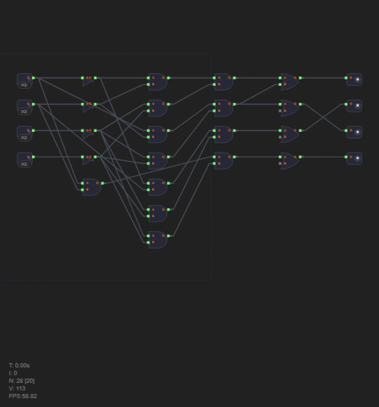
Level 44: Control Unit
Task
Implement an instruction decoder (Control Unit) — the key component of a processor that converts an operation code (opcode) into control signals.
The ControlUnit module accepts a 4-bit opcode and produces 4 control signals:
- RegWrite — register write enable (ADD, AND).
- MemWrite — memory write (STA).
- ALUSel — ALU operation select: 0=add, 1=AND.
- Branch — branch signal (JMP).
Recognized opcodes (mini-ISA):
| opcode | Instruction | RegWrite | MemWrite | ALUSel | Branch |
|---|---|---|---|---|---|
| 0 (0000) | ADD | 1 | 0 | 0 | 0 |
| 1 (0001) | AND | 1 | 0 | 1 | 0 |
| 2 (0010) | STA | 0 | 1 | 0 | 0 |
| 3 (0011) | JMP | 0 | 0 | 0 | 1 |
| 4–15 | NOP | 0 | 0 | 0 | 0 |
Use only AND, OR, NOT gates (structural approach). assign, if, case, always are forbidden.
Related materials
- System Pulse — instruction decoder in gate mode
- Verilog Is Not Programming — thinking in circuits
Solution for self-check
Try building the circuit yourself first. The solution below is a way to check yourself if you're stuck or have already solved it.
Contrast with software switch(opcode): a CPU compares the opcode step by step and picks a branch; in hardware it is a switching map where each AND detector instantly "recognizes" its code. Detectors do not think — they simply pass a signal when the bits match.
The decoder is built as detection trees for each opcode. Algorithm:
- Invert all opcode bits: n0 = NOT opcode[0], …, n3 = NOT opcode[3].
- Detect each opcode with an AND-tree of inverted/direct bits.
- Combine signals via OR for outputs active on multiple opcodes.
module ControlUnit(
    input wire [3:0] opcode,
    output wire RegWrite,
    output wire MemWrite,
    output wire ALUSel,
    output wire Branch
);
  wire n0, n1, n2, n3;
  not g0(n0, opcode[0]);
  not g1(n1, opcode[1]);
  not g2(n2, opcode[2]);
  not g3(n3, opcode[3]);

  // opcode=0 (ADD): all bits 0
  wire add_t1, add_t2, op_add;
  and ga1(add_t1, n0, n1);
  and ga2(add_t2, n2, n3);
  and ga3(op_add, add_t1, add_t2);

  // opcode=1 (AND): opcode[0]=1, rest 0
  wire and_t1, and_t2, op_and;
  and gb1(and_t1, opcode[0], n1);
  and gb2(and_t2, n2, n3);
  and gb3(op_and, and_t1, and_t2);

  // opcode=2 (STA): opcode[1]=1, rest 0
  wire sta_t1, sta_t2, op_sta;
  and gc1(sta_t1, n0, opcode[1]);
  and gc2(sta_t2, n2, n3);
  and gc3(op_sta, sta_t1, sta_t2);

  // opcode=3 (JMP): opcode[0]=1, opcode[1]=1
  wire jmp_t1, jmp_t2, op_jmp;
  and gd1(jmp_t1, opcode[0], opcode[1]);
  and gd2(jmp_t2, n2, n3);
  and gd3(op_jmp, jmp_t1, jmp_t2);

  // Outputs: OR combines opcodes
  or grw(RegWrite, op_add, op_and);
  or galusel(ALUSel, op_and, op_and);
  or gmem(MemWrite, op_sta, op_sta);
  or gbr(Branch, op_jmp, op_jmp);
endmodule
Total: 4×NOT, 12×AND, 4×OR. Each opcode is detected by three ANDs: two ANDs combine bit pairs, the third combines the results. Opcodes 4–15 activate no detector → all outputs = 0 (NOP).